COSMICDIAMONDS
Growing semiconductor-grade carbon from a levitating molten metal according to US Patent 12,716,147.
Everything silicon does, diamond does 10× better.
Diamond has the widest bandgap of any semiconductor, the highest thermal conductivity of any material, extreme chemical and radiation hardness, and nitrogen-vacancy centers operable at room temperature.
Quantum Technologies
- Defect centers in diamond act as the hard drive for quantum information storage.
- Nano-Tesla sensitivity enables jam-proof navigation using maps of Earth's magnetic fields.
Traditional / AI Compute
- Up to 120 GHz transistors with far less heat generation — a promising platform to push Moore's Law forward.
- ~5× better heat dissipation than any material; used today to cool high-end silicon chips, with commercial introduction in <2 years.
Lasers / Masers
- Produces more colors and power than any other Raman laser.
- First room-temperature continuous-wave solid-state masers (MRI, space communications).
Room-temperature quantum computing, sensing & advanced compute
Diamond is a foundational platform material for the 21st century — anchoring the next generation of compute and sensing infrastructure.
Power systems, electrochemistry, optics & lasers
When diamond prices fall dramatically, it reshapes nearly every industry — from wastewater to EVs, 5G/6G, renewables, and photonics.
Today's synthetic diamond will never rival silicon wafers.
CVD and HPHT — the only two growth methods that exist — are limited by first principles. Each trades one critical property for another. Electronic-grade diamond stays expensive, defect-prone, and small-scale — locked out of high-volume markets like CPUs, GPUs, and quantum information processing.
Chemical Vapor Deposition
- Co-grows atomic-scale graphitic defects that destroy crystal quality
- Growth rate capped at ~100 µm/hr (sparse plasma collisions)
- Prices ~1,000× electronic-grade silicon
High Pressure, High Temperature
- Chemical contamination from solid growth chamber & solvent metals
- Size-capped near 15 mm crystals
- Extreme pressures make tech-grade scaling impractical
Levitating Supersaturated Solution growth.
The first process to combine HPHT's crystallinity & speed with CVD's chemical purity — without their fundamental limitations, at atmospheric pressure.

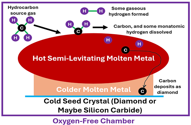
Levitating Supersaturated Solution (LSS) growth grows diamond from a levitating molten metal solution supersaturated with excess dissolved carbon. A diamond seed crystal contacts the supersaturated solution and withdraws downward as the boule grows, forcing the excess dissolved carbon to grow as diamond onto the seed — without the extreme pressures of HPHT. By growing from a levitating molten metal, HPHT-like crystallinity and growth rates are achieved; by removing chamber-wall contact, CVD-like chemical purity is achieved.
Dense liquid-metal environment yields ~1,000× more carbon-atom collisions than sparse plasma.
Solvent impurities segregate into initial growth layers — purity increases as the crystal grows.
No extreme forces. Far more practical and scalable than HPHT's gigapascal chambers.
Without chamber walls, all excess carbon is forced into the metastable diamond seed configuration.
A stepping-stone path from thermal grade to quantum.
Each product de-risks the next and funds it — minimizing capital needs while expanding the addressable market from ~$700M of tech-grade diamond toward $14B+.
Thermal-Grade Wafers
Niche Power Electronics & Optics
Initial >50 mm thermal-grade wafers sink heat from niche power-electronics chips and optical systems. Direct use of early boules is the lowest technical bar for commercial entry and builds process knowledge and early revenue.
BDD Electrodes
PFAS & Wastewater Treatment
Controlled boron doping creates electrochemical electrodes for on-site PFAS destruction, leveraging thermal-grade process learnings — priced below today's alternatives.
Scale to 300 mm
AI / HPC Wafer Bonding
Fab-compatible 300 mm diamond wafers bonded directly to commercial 300 mm AI/HPC wafers at the fab level — diamond has the highest thermal conductivity of any material.
Electronic & Quantum Grade
The Full Platform Unlocked
Electronic-grade power electronics and quantum sensing. Each phase de-risks and funds the next, approaching or surpassing silicon's $14B TAM.
The minds behind the breakthrough.
A multidisciplinary team spanning chemical engineering, MHD modeling, and materials science — backed by independent academic validation.

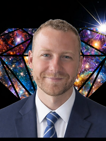
Steve Roys
B.S. Chemical Engineering, UIUC '18
Designed and built core systems enabling the first levitation-based diamond growth. Leads technical development from requirements to production with a strong background in fluid dynamics and heat transfer. Track record of designing, patenting and scaling manufactured products from the laboratory to mass production.

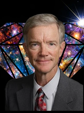
Dr. Edmund Seebauer
Prof. Emeritus, UIUC · Ph.D. Chem. Eng.
World-recognized expert in defect engineering and crystal growth kinetics. Provides senior validation that the observed growth behavior represents a true materials advance rather than a laboratory artifact. Also edits government grant applications.


Dr. Didzis Berenis
Lead MHD Researcher, Univ. of Latvia · Ph.D. Physics '23
Custom simulation code enables accurate prediction of levitated molten-metal behavior at scale. Broad background simulating many magnetohydrodynamic (MHD) flows across many fields informs Cosmic's levitator design decisions.
De-risked. Defensible. Proven.
The core physics is proven. The hardest technical hurdle is solved in simulation. The IP is granted and defensible. What remains is a milestone-driven path from prototype to product.
Proof-of-Concept Diamond Grown
Garage-scale prototype · UIUC
Clear crystalline diamond survived boiling nitric acid & lye. SP³ carbon signatures confirmed via Raman spectroscopy at UIUC — independently validated by Dr. Edmund Seebauer.
5 kg Semi-Levitation Solved in Simulation
3D two-phase MHD modeling · complete
Prior state of the art: 50 g continuous or 0.5 kg for minutes. Cosmic's breakthrough combines advanced multi-physics modeling on a dedicated supercomputer with proprietary coil geometries and heat-sink designs. The seed round funds the physical prototype.
US Patent Granted
US 12,716,147
US Patent 12,716,147 granted — protecting the core LSS process and apparatus. The patent is evergreen with an open continuation, while deep trade secrets in coils, chemistry, and modeling provide a five-year head start.
Semi-Levitation Prototype Proof of Concept
$500K seed · $12M post-money cap
A working open-air 5 kg proof-of-concept system, validated by x-ray photos. Completion marks the $76M valuation milestone.
Integrated Vacuum System Ready
Heat sink · vacuum chamber · controls
A fully integrated, temperature-controlled, inert-atmosphere vacuum system is ready for crystal growth, with 5 kg of target solvent semi-levitated at fixed temperature.
First Market-Ready Product
Thermal-grade or better
Targets >0.1 mm/hr growth, >50 mm OD diamond cylinders, and ≥1 kW/(m·K) thermal conductivity. Every remaining component is a well-understood industrial process, giving high confidence in this timeline.
From a $700M niche to a $14B platform.
A market constrained by CVD and HPHT cost and quality limits — confined to niche applications.
Cost improvements of 30×–621× across every diamond grade drive adoption beyond today's niche — approaching the electronic-grade silicon wafer TAM.
$500K seed at $12M post-money.
Milestone-driven capital de-risks the final hardware and carries Cosmic to a first product by end of 2028 — setting up high-valuation follow-on rounds as we step from a $700M niche toward a $14B+ platform.
At $12M post-money valuation cap.
Thermal-grade wafers or better.
Strategic sale, LBO, or IPO.
Request investor materials.
Request the full pitch deck, business plan, or schedule a founder meeting. All inquiries are reviewed directly by the founding team.